Process Introduction
—
Chapter 1: Introduction to Wafer Testing
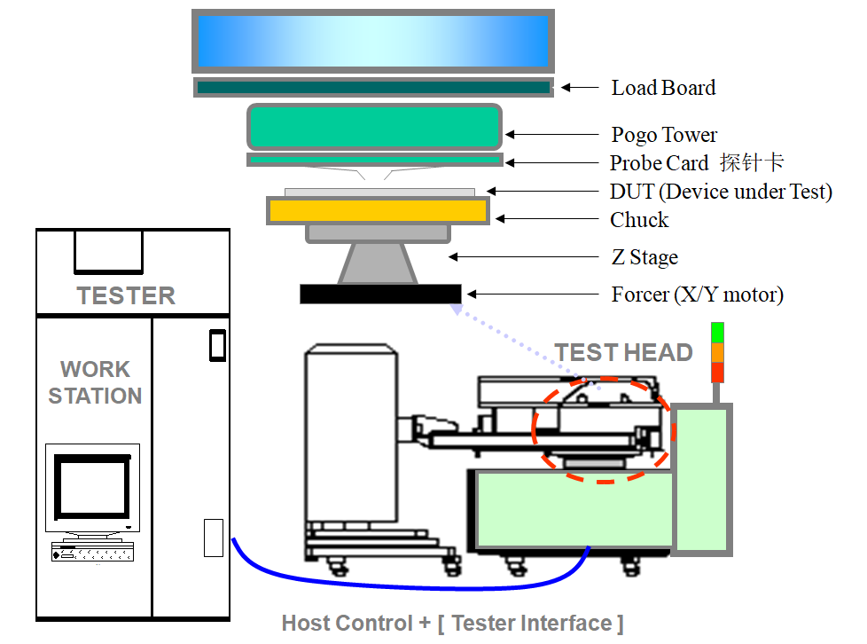
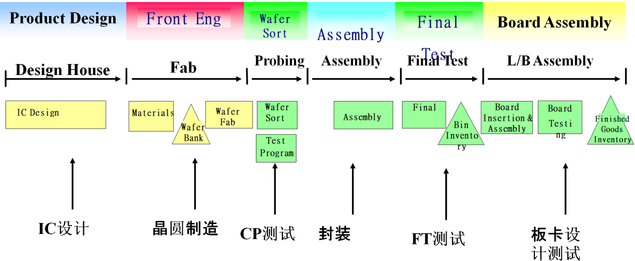
The method of wafer testing is mainly through the linkage of the testing machine (programmed in advance) and the probe station, relying on the contact connection of the probe card to perform wafer-level chip testing.
When the probe of the probe card correctly contacts the bondpads of each contact point of a die in the wafer, it sends a start signal to the tester tester through the test head Interface to start the test. The tester tester completes the test and sends back the classification signal (End of test) to the probe station Prober, and then the probe station Prober moves to the next test chip position. During mass production, the tester must be docked with the probe station probe to reciprocate in order to complete the test of a whole wafer.
Chapter Two, Wafer Test Equipment and Process
(1) Tester Tester: This is a test system for wafer testing. There are measurement units, control units, etc. in the tester. Engineers need to write a test language according to the spec and process of the customer's test chip in the engineering state. The languages of different types of test machines are also different. Test engineers need to master multiple languages and be proficient in the ability to call test machine resources. Each project product of each customer requires unique test programming, so test programming is also a process of software writing.
(2) Probe station Probe: This is a wafer carrying system. The main function is to load and unload wafers, and carry the wafers to move, so as to ensure that each product can be tested in every position. For the test of different products, the parameters of the probe station need to be debugged and recorded by the engineer in advance, and each chip is different. In addition, the accuracy of the probe station is very high, the accuracy of the XYZ axis is required to be at the nanometer level, and its moving accuracy and acceleration are adjustable. At the same time, the erection and calibration of the probe station are projects that test the ability of the test factory engineers. Horizontal and vertical accuracy, environmental temperature, environmental humidity, mold assembly accuracy, etc. all have absolute requirements.
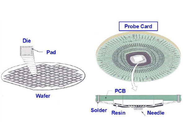
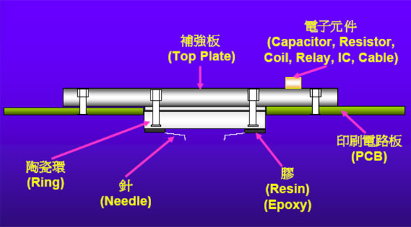
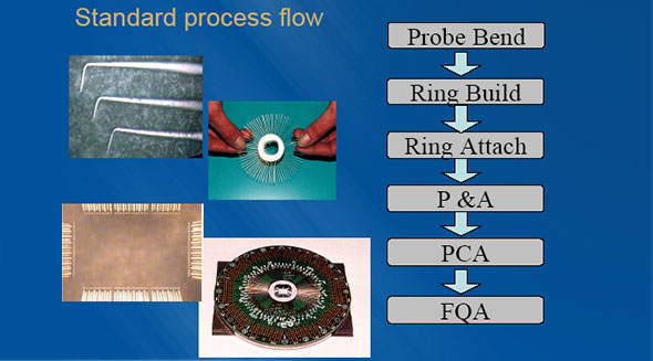
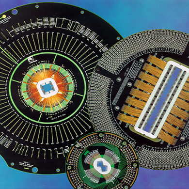
(3) Probe Card ProbeCard: This is a tool that connects the previous and the next. It is mainly responsible for linking the signal points of the tester and the chip BondPad.
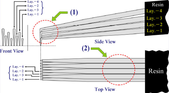
Traditional probe cards are divided into two types: cantilever type and vertical type. According to the customer's chip size, the chip pad size, whether there is a circuit under the pad, the needle pressure is controlled within 1-3 grams, chip overcurrent performance, chip compression performance, etc. It is the index parameter made by the probe card.
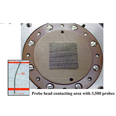
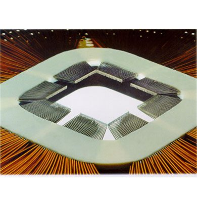
(4) Other process requirements: If the needle area cannot be greater than 25% of the chip area, the temperature is in the range of 25 degrees + -5 degrees, the humidity is between 40% and 60%, the environmental particles are less than 10,000 per cubic meter, and the surface area is 5 Point the needle to confirm to ensure the accuracy of the probe station, etc.
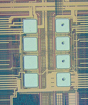
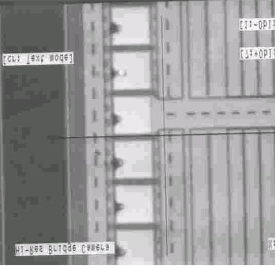
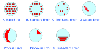
(5) After the test is completed, process analysis and test data transmission are required, mainly the transmission of MAP. Customers can understand the wafer test situation from the data.

Chapter Three: Design of Probe Card
(1) What is a pin card? PCB+pin+peripheral accessories
The relationship between the chip test and the pin card (the pin card is a passive fixture, which plays a role in the relationship between the tester signal and the chip Pad connection, the power socket on the PCB and the metal point are connected to the test signal of the tester, and the pin position under the PCB PAD connected to the chip)
(2) Notes and parameters for pin card design:
n Chip size, pad size Pay attention to the width of the dicing groove
n X,Y coordinate Pay attention to the customer layout, it is best to get the actual size, coordinate conversion and the same measurement conversion, X, Y, A, B, pad coordinates
n Notch front Pay attention to the actual notch of the wafer
n Pin assign Pay attention to the chip Pin parameters, signal type (power, ground, I, O, IO, analog signal, RF signal), simultaneous measurement influence and synchronization requirements
n Triangular printing direction Pay attention to the direction of the actual card holder position on the machine
n Needle height design pay attention to matching the external interface and Card Holder
n Needle layer design (PAD spacing and symmetry cause the needle card to be designed to be layered when the measured number is high)
(3) The testing standards for needle cards: the main testing parameters are as follows
• Offset Alignment
• Planarity
• Stitch Scrub
• Tip Diameter
• Contact Resistance
• Leakage
• Contact Force
(4) Problem judgment of ProbeCard
Needle problems (level, needle point, needle pressure, stitch length)
PCB problems (horizontal, orientation, internal circuit)
Peripheral circuit problems (capacitor resistance, Relay, other circuits)
Connection problem (socket, docking level)
Chapter Four, Wafer Test Cost
Factors that determine the cost of CP testing:
(1) Machine cosa) Machine configuration (IO quantity, analog/digital, voltage and current accuracy requirements)
b) Prober configuration (wafer size, mechanical time)
(2) Test tim
a) Test program time (test items, power-on time)
b) Same test quantity
c) TTR (Test Time Reduction), merge test items, test first with high coverage.
Chapter 5 Introduction to finished product testing
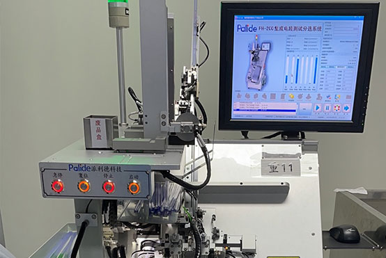
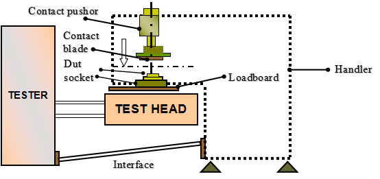
The method of finished product testing is mainly through the linkage of the testing machine (programmed in advance) and the manipulator, relying on the contact connection of the test socket Socket or golden finger, to carry out the finished chip test.
When the handler's arm puts the DUT into the socket, the contact pushor is pressed down, and after the DUT's feet are correctly in contact with the socket, it sends a start signal to the tester through the interface. After the test is completed, the tester sends back binning and EOT signals; the handler does Classification actions. Depending on the size and number of feet of the customer's products, the handler provides different kits for use. During mass production, the Handler must be combined with the tester and connected to the interfacer to test, so that a whole batch of chip tests can be completed by reciprocating.
Chapter Six, Finished Product Test Equipment and Process
(1) Tester Tester: This is a test system for finished product testing. There are measurement units, control units, etc. in the tester. Engineers need to write a test language according to the spec and process of the customer's test chip in the engineering state, each type The language of the test machine is also different. The test engineer needs to master multiple languages and be able to master the ability to call the resources of the test machine. Each project product of each customer requires unique test programming, so test programming is also a process of software writing.
(2) Manipulator Handler: This is the system carried by the chip. The main function is to introduce the chip into the test fixture on the fixed track, and carry the chip to move, so as to ensure that each product can be tested. For the test of different products, there are different package outline PODs, and different fixtures and Handlers need to be selected according to the outline size of the chip to complete. There are gravity type, turret type, and translation type.
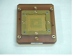
(3) Test socket Socket: This is a tool for chip connection, which is mainly responsible for linking the signal points of the test machine and the signal points of the external pins of the chip. According to the size requirements and appearance requirements of different chips and the number of pins, the test sockets should also be matched with each other.
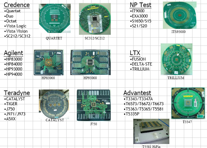
(4) Test connection board Loadboard: This is a tool that connects the previous and the next. It is mainly responsible for linking the signal points of the test machine and the signal points of the test socket. Depending on the connection of the external signal of different test machines, and the size and connection of the test base, the connection points of the Loadboard should also be matched accordingly.
(5) After the test is completed, process analysis and test data transmission are required, mainly the transmission of Summary. Customers can understand the yield of the finished product test from the data
Chapter 7: Finished product testing cost
Factors that determine the cost of FT testing:
(1) Machine cost
a) Machine configuration (IO quantity, analog/digital, voltage and current accuracy requirements)
b) Handler configuration (chip size, mechanical time UPH)
(2) Test time
a) Test program time (test items, power-on time)
b) Same test quantity
c) TTR (Test Time Reduction), merge test items, test first with high coverage.
Chapter 8 Technical Threshold of Wafer Testing and Finished Product Testing Industry
The core DNA of the semiconductor testing industry is based on a variety of high-precision and high-efficiency automation equipment and high-precision hardware, relying on the core high-end talents' test program development and debugging capabilities and process quality analysis capabilities to provide customers with tailor-made semiconductors Wafer testing service solutions.
(1) Understand and proficient in the use of advanced test system Tester
(2) Proficient in control and maintenance of advanced probe station system Prober and manipulator system Handler.
(3) Reasonably design probe card and load board and proficient in maintenance
(4) Development and debugging of test programs for core competitiveness
(5) Stable factory environment and power system maintenance
(6) Proficient in process quality analysis and big data management analysis ability
Chapter Nine, Semiconductor Testing Industry Requirements
1. Tester system (hardware):
The mainstream testing machines for semiconductor testing are all imported, and after many years of evolution and technology accumulation, foreign testing machines have grown from a hundred flowers to only a few influential testing machine suppliers, and the choices are gradually reduced. With the gradual increase in the requirements of test chips, from the test requirements for current, voltage, and resistance, to the later requirements for functions, frequency, AD\DA, etc., the test unit of the tester is becoming more and more complex, and the update of the tester is also Gradually speed up, the test hardware boards and test software systems of different test machines are not the same. Test engineers need to constantly update the knowledge of the test machine, learn the architecture and software characteristics of the new test machine, and choose the cost-effective product that suits the customer. Test machine system.
2. Probe station system Prober (hardware):
The probe station used for semiconductor wafer testing is mainly imported equipment from Japan, which is high-precision integrated automation equipment. Because the chip size is as small as nanometers, the precision of the probe station is extremely high. The precision requirements such as X axis, Y axis and Z axis all reach the nanometer level. Therefore, the materials and precision processing and assembly technology used to manufacture the probe station are beyond the reach of the domestic basic industry. The use of the probe station also needs to tailor the variety parameters for each subdivided product of the wafer test customer. At the same time, the maintenance and calibration work in the usual test phase is also an extremely professional project. The high-precision, high-stability operation of the probe station is directly related to the accuracy and productivity of wafer testing.
3. Probe card (hardware):
The probe cards for semiconductor wafer testing are dedicated probe cards, and the probe cards for each product of each customer are different. Before professional card making, you need to communicate various technical details with customers, including probe material, probe size, chip size, cutting lane width, needle penetration depth, needle penetration strength, aluminum layer thickness, and the number of simultaneous measurements. Probe cards are consumables for wafer testing. Reasonable design and use of probe cards, timely maintenance and maintenance can improve the life and test efficiency of the probe cards, and reduce the cost of wafer testing. Equipped with professional on-site probe card maintenance personnel, which can effectively control the test quality. The test stability and maintenance ability of the high-test probe card is also the core technology of semiconductor wafer testing.
4. Handler of the manipulator system (hardware):
The manipulators used in the testing of semiconductor products are mainly domestic and imported equipment, and are high-precision integrated automation equipment. Depending on the package shape of the customer's product, the required accuracy of the manipulator is also different. In addition, the hourly operating speed UPH of the manipulator directly determines the accuracy and speed cost of the manipulator.
5. Load board (hardware):
The Loadboard of the finished semiconductor test uses a dedicated board, and each Loadboard of each test machine is different. Before professional manufacturing, it is necessary to communicate various technical details with customers, including chip packaging form, size, tester signal distribution, Socket signal distribution, simultaneous measurement quantity, etc.
6. Test program development and debugging (software):
The core software technology of semiconductor testing is the development and debugging of test programs. From the beginning of the project to mass production, the customer's products must go through the design plan, probe card design and production, test program development, test program debugging, trial production, number machine development, small-scale mass production and other steps. Among them, the development and debugging of test programs are the core links that test engineers' understanding of testing machines and products, test the ability of writing and developing test software, and test the understanding of process debugging. At the same time, being able to provide safe, stable and efficient test solutions and have good communication and interaction with customers is also the key to test program development and debugging. The higher the test program development of the same test, the more reasonable the software is written, and the higher the efficiency and accuracy of the algorithm.
7. Factory environment and power system (hardware):
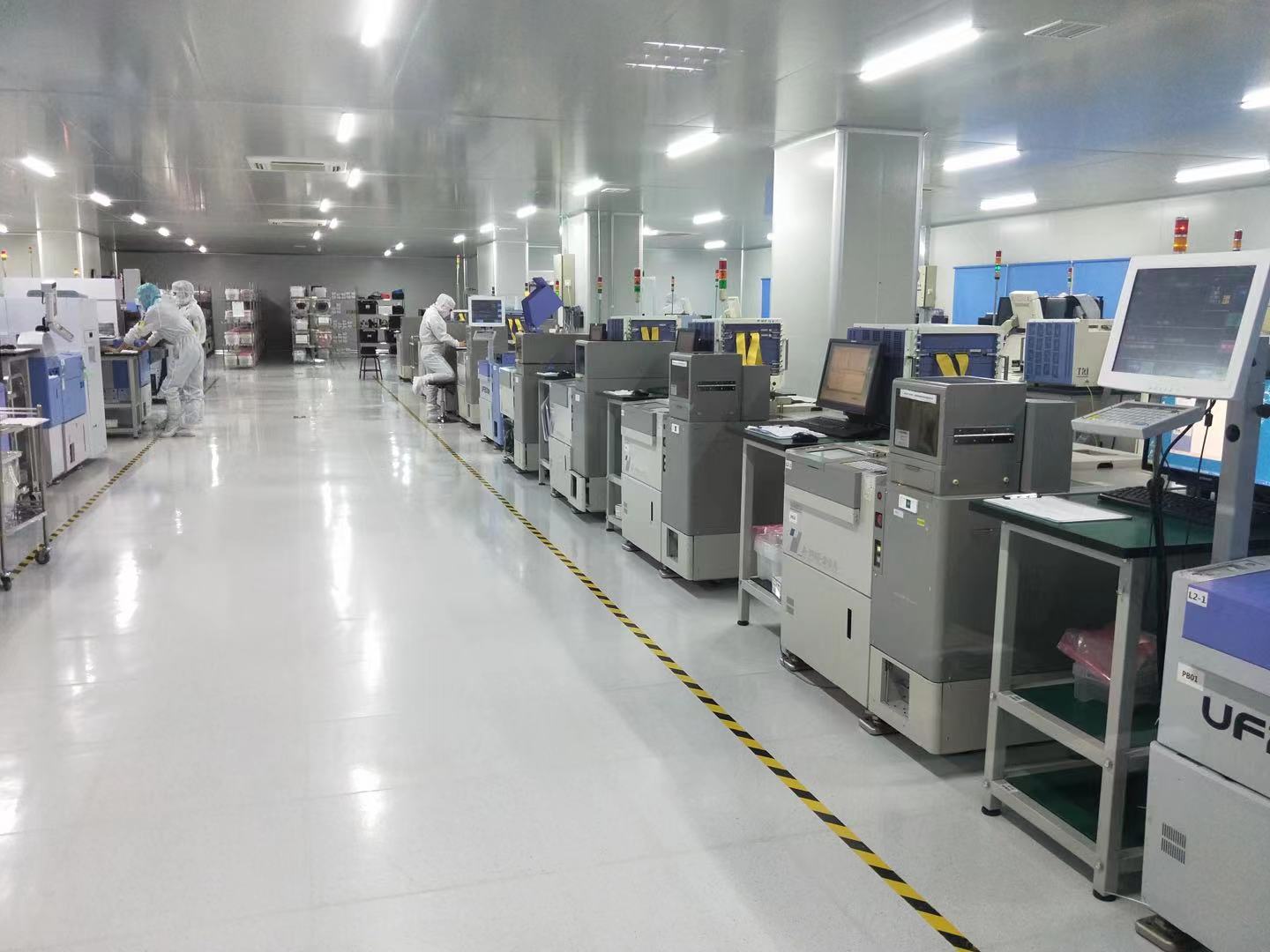
The factory environment for semiconductor testing is very demanding, and the amount of dust per cubic meter must be controlled within 10,000. In the design process of the plant, it is necessary to consider the level of air-conditioning filtration, the wind force and direction of each air outlet and return air outlet, and the pressure, temperature and humidity inside the factory must also be strictly controlled. Since both the testing machine system and the probe station system require stable electrical energy, stable positive air pressure, and negative air pressure, the construction and maintenance of the power system of the entire plant is also the basis for stable mass production.
8. Process quality analysis and data management analysis (software):
The link of semiconductor wafer testing is an intermediate step between wafer manufacturing and packaging. It is an important process control link for supervising wafer manufacturing yield. Therefore, proficiency and understanding of domestic mainstream wafer manufacturing processes are also necessary skills for wafer testing. In this way, the defects of the process can be found in time in the wafer test process and results to improve the yield of the wafer manufacturing plant, thereby reducing the loss of customers.
The test of semiconductor products is an intermediate step between packaging and chip sales. It is an important process control link that supervises the packaging yield. In addition, since the wafers and finished products tested every day are countless, a good server system, big data analysis and management capabilities are also necessary for the testing industry. When the customer needs to trace the product data, it can provide timely, effective and accurate data, and convert it into the format required by the customer, so as to facilitate the analysis of problems and provide decision-making.
